EEVblog #1216 - PCB Layout + FPGA Deep Dive
Only Dave can turn a simple question into a 1hr deep dive monologue into PCB layout and FPGA implementation.
FPGA power supplies, DC margins, dynamic power requirements, power budgets, high power designs, multi layer PCB design, placement, system considerations, power planes, copper weighting, stackups, routing, split planes, star grounding, blind and buried vias, high speed traces, return paths, EMC, and a whole lot more.
BGA Fanout Tutorial:
IBM T221 Monitor Teardown:
Bypass Capacitors Visualised:
Forum: /
#FPGA #PCB #Design
Bitcoin Donations: 38y7DE8HEHNj8fGDtUr4PkCn9nWxiorvvy
Litecoin: ML7oQokTwB38bgzzjLDbRV97HKAHuwRfHA
Ethereum: 0x11AceA38DCA9DbFfB4F35f3F746af65F9dED28ce
EEVblog Main Web Site:
The 2nd EEVblog Channel:
Support the EEVblog through Patreon!
AliExpress Affiliate:
Buy anything through that link and Dave gets a commission at no cost to you.
Stuff I recommend:
/
Donate With Bitcoin & Other Crypto Currencies!
/
T-Shirts:
Likecoin – Coins for Likes:
Recipes
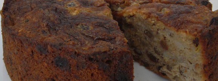
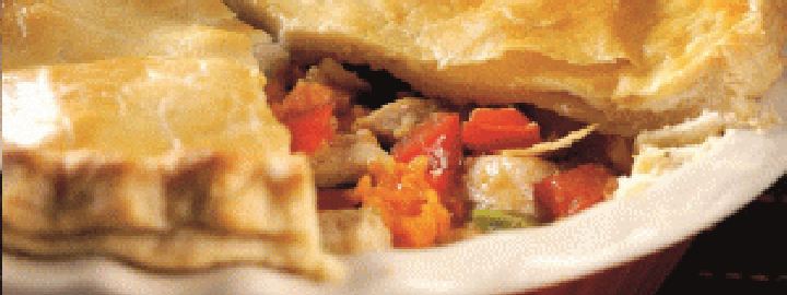
Savoury recipes
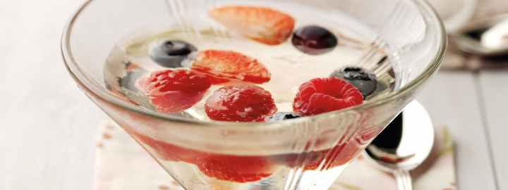
Pumpkin pie
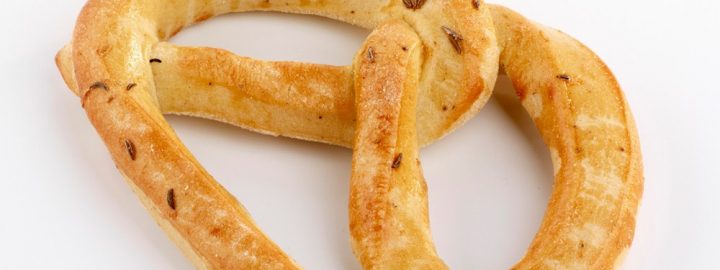
Hand baked bread recipes
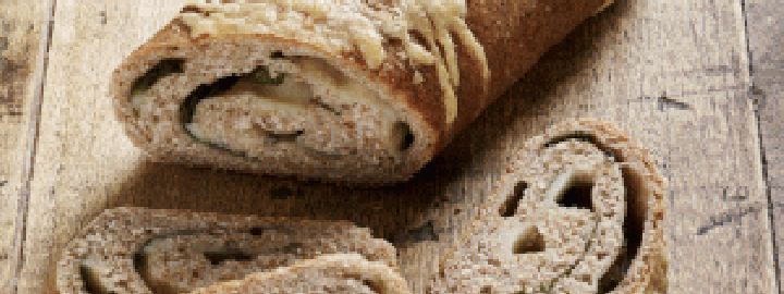
Pretzel with caraway seeds
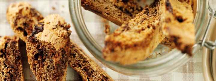
Biscuit recipes
Honeycomb and milk chocolate biscotti

Cupcake recipes
Cointreau and chocolate mini cupcakes
Sweet dough recipes
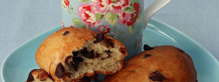
Chocolate chip brioche
Hand baked bread recipes